YIC EMProbe DBM Overview
EMProbe: 1,218 H-field probes
Accurate and Repeatable High-Resolution EMC and EMI diagnostic with Handheld Near Field Probes on your lab-bench
EMC/EMI issue testing is straightforward and accurate with 3D precision technology.
Used to assist high-density board designers to use off-the-shelf hand-held probes and visualize the root causes of potential EMC and EMI problems during pre and post-EMC compliance testing.
Product Features
Capability:
Spectral scan, spatial scan, peak-hold, continuous scanning, spectral and spatial comparison, scripting, limit lines, report generation, and notes.
Spatial scan time:
Continuous real-time for the entire scan area (1,218 probes activated) when Level 1 is selected: 5 sec.
Selected area 2.25 cm x 2.25 cm, 9 probes activated.
Level 1: <0.5 sec. | Level 2: 4 sec. | Level 3: 9 sec. | Level 4: 21 sec. | Level 5: 55 sec. | Level 6: 2 min 35 sec. | Level 7: 7 min 23 sec. | Level 8: 24 min 00 sec.
Spectral scan time:
11 seconds for L 10 cm x W 10 cm (L 4" x W 4", 178 probes activated) from 10 MHz span to 110 MHz and 122 kHz RBW. Scanning area, span, and RBW are user selectable within spectrum analyzer specifications
Supported operating systems:
Windows 10®
Supported overlays:
Picture in JPEG format
Standard Gerber© RS274x format and HPGL format CAD files
Specifications
Broadband frequency coverage:
Base configuration = 150 kHz to 8 GHz
Antenna array:
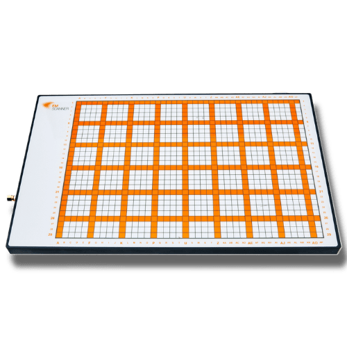
1,218 (42 x 29) H-field probes.
Spatial resolution:
Level 1: 7.50 mm | Level 2: 3.75 mm | Level 3: 1.88 mm | Level 4: 0.94 mm
Level 5: 0.47 mm | level 6: 0.24 mm | Level 7: 0.12 mm | Level 8: 0.06 mm
Scan area:
L 31.6 cm x W 21.8 cm (L 12.44" x W 8.58")
The frequency accuracy of peaks:
Peak marking accuracy of the spectrum analyzer
Probe to probe uniformity:
Calibrated before shipment. Firmware correction factors adjust for frequency-dependent probe responses with +/- 3 dB accuracy
Measurement plane isolation:
> 20 dB
Maximum radiated power load:
10 W / 40 dBm
Enclosure:
Anodized non-conductive metal
Maximum DUT voltage:
Glass Cover: 4kV DC; 2.6kV AC | Metal Case: 260V DC; 200V AC (measured as dielectric withstanding voltage - DWV)
Operating temperature:
From 15° C to 40° C
Fuse Rating:
8A
Scanner connections:
PC: Ethernet
Dimensions of the scanner:
L 34.5 cm x W 43.5 cm x H 11 cm (L 13.58 x W 17.13" x H 4.33")
Weight:
12.70 Kg / 28 lb (including cables and the adapter)
Using Handheld probes to identify and resolve EMC/EMI issue testing has never been this accurate. 3D Precision Technology used to assist high density board designers to use off the shelf hand-held probes and visualise the root causes of potential EMC and EMI problems during pre and post EMC compliance testing.
EMC and signal integrity are major concerns in the design of high-speed PCBs. While EMScanner allows designers to easily locate emission by placing the PCB on its flat surface, the EMProbe allows users to test the component side of the PCB and adjust the height of the scan.
This enables the design engineers to diagnose EMC/EMI problems limited only by the choice of the Spectrum Analyzer and the Near Field Probe and allows them to visualize the root causes of potential EMC and EMI problems of a non-flat surface or of a complete product.
During any new product development process, design engineers must find, characterize, and address unintended radiators or RF leakage to pass compliance testing. EMProbe allows board designers to pre-test and resolve EMC and EMI problems early on, thus avoiding unexpected EMC compliance test results.
EMProbe delivers repeatable and reliable results that pinpoint the cause of a design failure.
As a result, the user can personally test the design without having to rely on another department, test engineer, or time-consuming off-site testing. After diagnosing even an intermittent problem, the engineer can implement a design change and retest. The results provide concrete verification of the effectiveness (or not) of the design change.
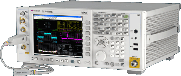
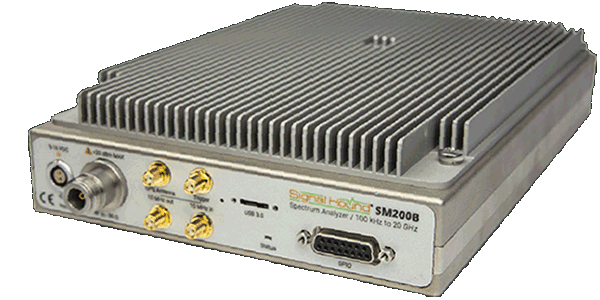
The EMProbe solution consists of a computer controlled Robotic Arm, Near Field probe and a customer-supplied Spectrum Analyzer, all controlled by the included EMViewer SW.
The EMProbe diagnostic capabilities allow design teams to reduce testing time by more than two orders of magnitude. Users have also documented fifty percent reductions in design cycle times. This allows the design team to immediately analyse and compare design iterations.
Ideal projects for the EMProbe are components side testing of boards designed for high speed, high power, and/or high density/complexity. Any PCB that places a premium on board real-estate also qualifies as an excellent candidate.
The EMProbe provides an easy-to-use, cost-effective, and scalable solution for design teams. Emission, immunity, filtering, EMI shielding, broadband noise and Common Mode testing are some of the applications that the EMProbe system addresses in mere seconds.
YIC Technologies’ EMProbe How-To Videos
VIDEO
